(Credit: Credit: Queen’s University Belfast)
Queen’s University Belfast researchers have discovered a new way to create extremely thin electrically conducting sheets, which could revolutionise the tiny electronic devices that control everything from smart phones to banking and medical technology.
Through nanotechnology, physicists Dr. Raymond McQuaid, Dr. Amit Kumar and Professor Marty Gregg from Queen’s University’s School of Mathematics and Physics, have created unique 2-D sheets, called domain walls, which exist within crystalline materials.
The sheets are almost as thin as the wonder-material graphene, at just a few atomic layers. However, they can do something that graphene can’t – they can appear, disappear or move around within the crystal, without permanently altering the crystal itself.
This means that in future, even smaller electronic devices could be created, as electronic circuits could constantly reconfigure themselves to perform a number of tasks, rather than just having a sole function.
Professor Marty Gregg explains: “Almost all aspects of modern life such as communication, healthcare, finance and entertainment rely on microelectronic devices. The demand for more powerful, smaller technology keeps growing, meaning that the tiniest devices are now composed of just a few atoms – a tiny fraction of the width of human hair.”
(Credit: Credit: Queen’s University Belfast)
“As things currently stand, it will become impossible to make these devices any smaller – we will simply run out of space. This is a huge problem for the computing industry and new, radical, disruptive technologies are needed. One solution is to make electronic circuits more ‘flexible’ so that they can exist at one moment for one purpose, but can be completely reconfigured the next moment for another purpose.”
The team’s findings, which have been published in Nature Communications, pave the way for a completely new way of data processing.
Professor Gregg says: “Our research suggests the possibility to “etch-a-sketch” nanoscale electrical connections, where patterns of electrically conducting wires can be drawn and then wiped away again as often as required.
“In this way, complete electronic circuits could be created and then dynamically reconfigured when needed to carry out a different role, overturning the paradigm that electronic circuits need be fixed components of hardware, typically designed with a dedicated purpose in mind.”
(Credit: Credit: Queen’s University Belfast)
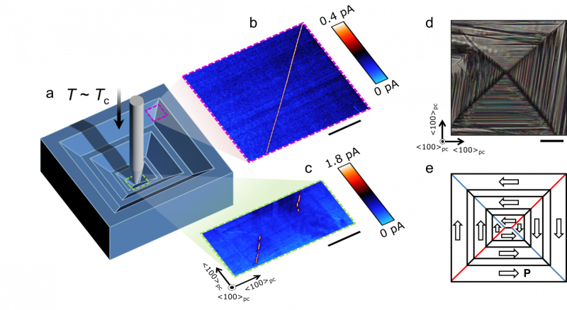
There are two key hurdles to overcome when creating these 2-D sheets, long straight walls need to be created. These need to effectively conduct electricity and mimic the behavior of real metallic wires. It is also essential to be able to choose exactly where and when the domain walls appear and to reposition or delete them.
Through the research, the Queen’s researchers have discovered some solutions to the hurdles. Their research proves that long conducting sheets can be created by squeezing the crystal at precisely the location they are required, using a targeted acupuncture-like approach with a sharp needle. The sheets can then be moved around within the crystal using applied electric fields to position them.
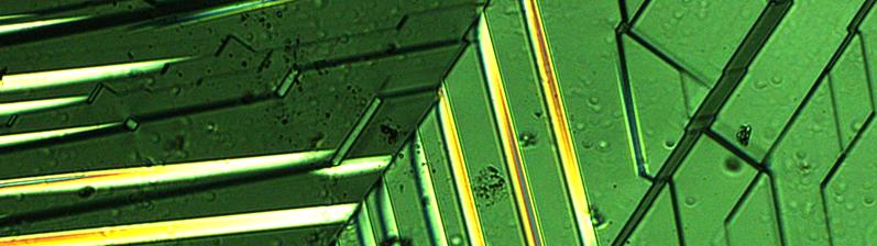
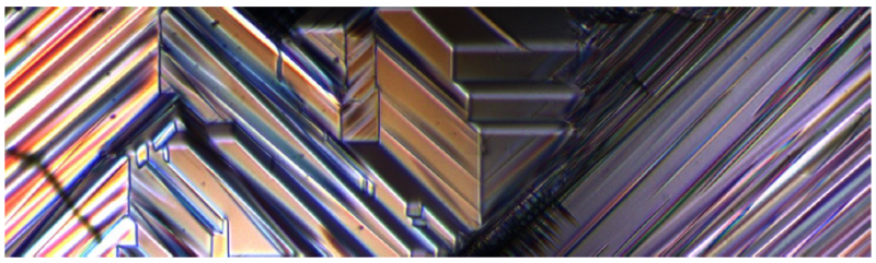
Dr. Raymond McQuaid, a recently appointed lecturer in the School of Mathematics and Physics at Queen’s University, adds: “Our team has demonstrated for the first time that copper-chlorine boracite crystals can have straight conducting walls that are hundreds of microns in length and yet only nanometres thick. The key is that, when a needle is pressed into the crystal surface, a jigsaw puzzle-like pattern of structural variants, called “domains”, develops around the contact point. The different pieces of the pattern fit together in a unique way with the result that the conducting walls are found along certain boundaries where they meet.
“We have also shown that these walls can then be moved using applied electric fields, therefore suggesting compatibility with more conventional voltage operated devices. Taken together, these two results are a promising sign for the potential use of conducting walls in reconfigurable nano-electronics.”