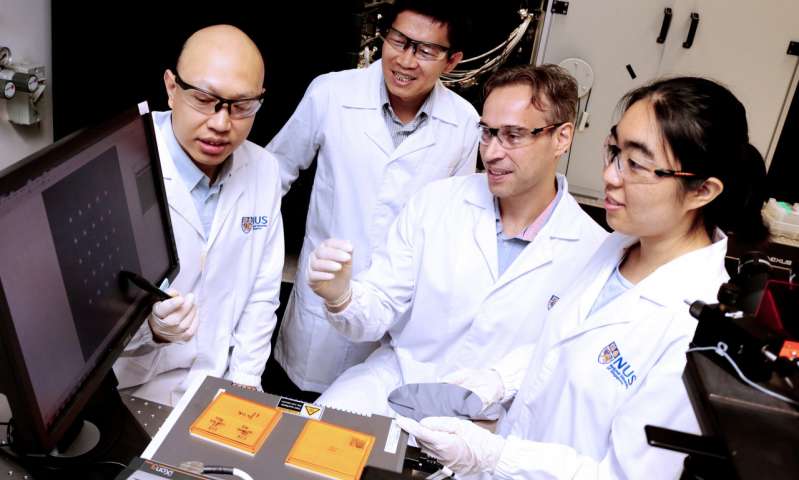
A research team led by Associate Professor Christian Nijhuis from the Department of Chemistry at the NUS Faculty of Science (second from right) has recently invented a novel “converter” that can harness the speed and small size of plasmons for high frequency data processing and transmission in nanoelectronics. (Credit: National University of Singapore)
A research team from the National University of Singapore has recently invented a novel “converter” that can harness the speed and small size of plasmons for high frequency data processing and transmission in nanoelectronics.
Advancement in nanoelectronics, which is the use of nanotechnology in electronic components, has been fueled by the ever-increasing need to shrink the size of electronic devices in a bid to produce smaller, faster and smarter gadgets such as computers, memory storage devices, displays and medical diagnostic tools.
While most advanced electronic devices are powered by photonics – which involves the use of photons to transmit information – photonic elements are usually large in size and this greatly limits their use in many advanced nanoelectronics systems.
Plasmons, which are waves of electrons that move along the surface of a metal after it is struck by photons, holds great promise for disruptive technologies in nanoelectronics. They are comparable to photons in terms of speed (they also travel with the speed of light), and they are much smaller. This unique property of plasmons makes them ideal for integration with nanoelectronics. However, earlier attempts to harness plasmons as information carriers had little success.
Addressing this technological gap, a research team from the National University of Singapore (NUS) has recently invented a novel “converter” that can harness the speed and small size of plasmons for high frequency data processing and transmission in nanoelectronics.
“This innovative transducer can directly convert electrical signals into plasmonic signals, and vice versa, in a single step. By bridging plasmonics and nanoscale electronics, we can potentially make chips run faster and reduce power losses. Our plasmonic-electronic transducer is about 10,000 times smaller than optical elements. We believe it can be readily integrated into existing technologies and can potentially be used in a wide range of applications in the future,” explained Associate Professor Christian Nijhuis from the Department of Chemistry at the NUS Faculty of Science, who is the leader of the research team behind this breakthrough.
This novel discovery was first reported in the journal Nature Photonics on 29 September 2017.
From electricity to plasmons in one single step
In most techniques in plasmonics, plasmons are excited in two steps – electrons are used to generate light, which in turn is used to excite plasmons. To convert electrical signals into plasmonic signals, and vice versa, in one single step, the NUS team employed a process called tunnelling, in which electrons travel from one electrode to another electrode, and by doing so, excite plasmons.
“The two-step process is time-consuming and inefficient. Our technology stands out as we provide a one-stop solution for the conversion electrical signals to plasmonic signals. This can be achieved without a light source, which requires multiple-steps and large optical elements, complicating integration with nanoelectronics. Based on our lab experiments, the electron-to-plasmon conversion has an efficiency of more than 10 per cent, more than 1,000 times higher than previously reported,” added Assoc Prof Nijhuis, who is also from the NUS Centre for Advanced 2-D Materials and NUS Nanoscience and Nanotechnology Institute.
This groundbreaking work was conducted in collaboration with Dr. Chu Hong Son from the Institute of High Performance Computing under the Agency for Science, Technology and Research.
The researchers plan to conduct further studies to reduce the size of the device so that it can operate at much higher frequencies. The team is also working on integrating the transducers with more efficient plasmonic waveguides for better performance.