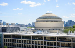
MIT’s Materials Research Laboratory, seen here in front of the MIT dome, will house the new Materials Research Science and Engineering Center.
[Photo courtesy of Gretchen Ertl]
The center will focus on advanced materials science for medical imaging, sustainable metals production and next-generation semiconductors, the university said.
The NSF is expected to provide $18 million over six years in research funding to the center. At the time of publication, the funding is pending MIT’s negotiation of a formal research agreement with the agency, the university said.
“The long-term goal is for the broader materials and engineering community to see the disruptive potential of bringing researchers together across disciplines to solve complex challenges,” MIT Associate Professor Rafael Jaramillo said in a news release. “And that includes specifically in medical diagnostics and metals production, where entirely new things will be possible that aren’t considered possible today.”
Related: This researcher’s development could inspire new and next-gen neuromod technologies
MIT’s new research hub will mainly focus on two research areas. One research arm will focus on developing specialized materials for better X-ray detectors, technology that could sharpen medical imaging, improve cancer diagnosis technology, cut radiation doses and strengthen industrial and security scanning.
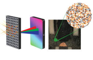
An illustration of a nanostructured scintillator converting X-ray radiation into visible light. [Illustration courtesy of Rafael Jaramillo]
MIT’s second research path will work with high-temperature sulfur-based molten materials, aiming to redesign how semiconductors are made. In doing so, these researchers could develop ways for “more efficient metal production, improved access to critical materials and new thin-film semiconductor technologies,” the university said.
The award is part of a $108 million investment from the NSF Materials Research Science and Engineering Centers program divided between six new research centers focused on materials science and engineering. MIT joins the University of California, San Diego, Princeton University, Harvard University, Columbia University and the University of Nebraska-Lincoln as investment recipients.
Across all six centers, NSF expects the funding to support more than 250 undergraduates, upward of 150 graduate students and over 60 early-career researchers.
“We were inspired to continue that legacy of collaborative research in materials science,” Jaramillo said. “It’s mainly the mode of working — the mode of working in a very intentional way as a team across disciplinary boundaries and having this program that brings people together.”