Numerous types of sensors are used in medical devices and systems to enhance product efficiency, accuracy and reliability. They range from extremely small sensors to large load cells; the most complicated tend to be those used in implantables and medical systems, and include “touch-feedback” applications that are required for efficient and safe robotic surgery.
The common requirement for all these sensors is their need for protection to ensure the reliable life of medical devices. This protection cannot always be built into the structure of the overall device and may need to be handled on the component level. To keep pace with the critical sensor protection needs, medical device designers can take a hand from NASA. Parylene has been the preferred component protection for electronics used in space exploration and aerospace systems for decades. Parylene has also become the protection of choice for many medical devices, systems and components for several key reasons: it is extremely lightweight, almost impossible to penetrate, biocompatible and biostable.
Understanding the Parylene Difference
Parylene is the name for a group of organic poly (para-xylylene) polymers often used as moisture and dielectric barriers. What differentiates the Parylenes from many other types of conformal coatings is that they are applied by vapor deposition—not via spraying, dipping, brushing or dispensing. They are deposited as a gas in a process that does not rely on line-of-sight physics. The polymer literally “grows” on device surfaces at a molecular level, which means they provide uniform, conformal coverage of all component surfaces, even penetrating into the smallest crevices to provide a complete, biocompatible barrier that is only microns thick (Figure 1).
 vs. Liquid (bottom) comparison.jpg)
Figure 1. The polymer literally “grows” on device surfaces at a molecular level, which means they provide uniform, conformal coverage of all component surfaces, even penetrating into the smallest crevices to provide a complete, biocompatible barrier that is only microns thick.
Devices to be coated with Parylene are placed in a room-temperature deposition chamber. A powdered raw material, known as dimer, is placed in the vaporizer at the opposite end of the coating system. The double-molecule dimer is heated, sublimating it directly to a vapor, which is then rapidly heated to a very high temperature (~680° C) that cracks (pyrolizes) it into a monomeric vapor. This vapor then travels into an ambient temperature deposition chamber where it spontaneously polymerizes onto all surfaces, forming the ultra-thin, uniform, and extremely conformal Parylene film. The entire Parylene coating process is carried out in a closed system under a controlled vacuum. The deposition chamber (Figure 2) and items to be coated remain at ambient temperature throughout the entire process. No additional cure process or steps are required.
Parylene is typically applied in thickness ranging from 500 angstroms to 75 microns, maintaining excellent properties in ultra-thin films. A 25 micron coating, for example, will have an electrical insulating capability of up to 7,000 volts. No other coating material can be applied as thin as Parylene and still provide the same level of protection. The molecular “growth” of Parylene coatings ensures not only a uniform conformal coating at the thickness specified by the manufacturer, but because formed from a gas, its deposition ensures complete encapsulation of all surfaces without blocking or bridging small openings.
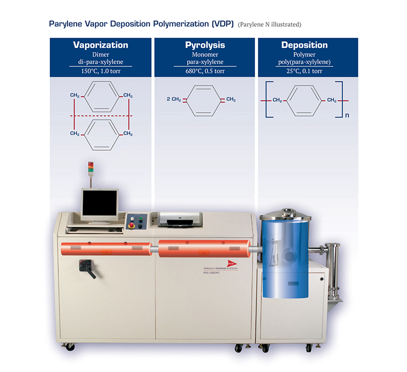
Figure 2. A deposition chamber for Parylene.
Parylene variants are free of fillers, stabilizers, solvents, catalysts, and plasticizers. As a result, the coating presents no leaching, outgassing or extraction issues. Their naturally low coefficient of friction provides dry-film lubricity properties that benefit moving parts, including syringe and infusion device applications, eliminating the need for silicone oils that are often used as a lubricant in syringe-type devices. For implanted devices, Parylene provides components with both biocompatibility and biostability.
A key feature of Parylene for any sensor-based medical implantable device or system is their ultra-thin film delivers necessary protective benefits without compromising the mechanical or functional attributes of the sensor, the device, or signal transmissions—regardless of how small it is—while ensuring biocompatibility within the body. That is a key issue for the latest in MEMS sensors. For devices requiring electrical communication, Parylene provides low dielectric constants and dissipation factors.
There are three common variants of Parylene commercially available for the medical device industry: Parylenes N, C, and Parylene HT. Each Parylene has unique properties that make it advantageous for medical device and sensor applications. All three Parylene formulations are biocompatible and biostable per ISO-10993 and USP Class VI biological evaluations, and all are compatible with today’s common sterilization methods (e.g. e-beam, gamma, EtO, peroxide plasma, steam autoclave, etc.) Figure 3 shows the properties of Parylene for medical applications.
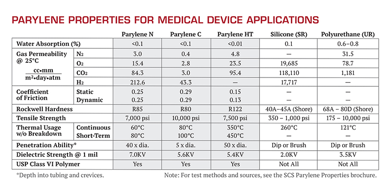
Figure 3. Typical properties of Parylene for medical applications.
Application Examples
Dick Molin is Medical Market Segment Manager for Specialty Coating Systems, a provider of Parylene coating services and technologies. His forté is understanding medical design engineers and their needs, and also being able to provide a materials perspective, working with them on various applications—not only from a functional standpoint, but to enhance reliability of their devices as well.
According to Molin, most sensors comprise materials that are not naturally compatible with the human body. For example, some of the more advanced sensors being developed are now silicon–based, a material that can have deleterious effects on the body long-term. In addition to biocompatibility issues, protective solutions must also function properly at high frequencies as communications move up and down the chain. Some Parylene formulations have been tested up into and beyond the 6 GHz range. Additionally, most Parylene formulations conform to the IPC (Institute for Interconnecting and Packaging Electronic circuits) standards for conformal coatings, which supersede the military standard MIL-I-46058 that characterizes coatings up to 1MHz.
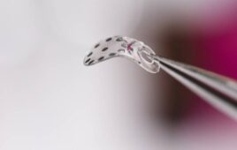
According to Molin, some common applications of Parylene include protecting electronics and sensors in all types of implantable medical devices, particularly in the areas of embedded stimulation such as cardio and neurostimulation. For instance, pacemakers have long been coated with Parylene (Figure 4). These types of devices require full biocompatibility with failsafe operation and signal protection. Parylene does not add significant dimensions to components and transferred signals remain strong and clear, factors important to the increased use of highly miniaturized sensor assemblies in robotic surgical systems.
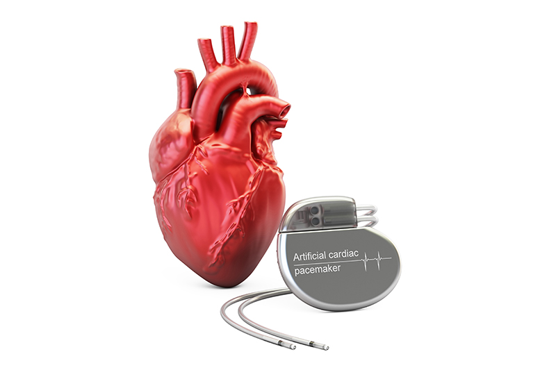
Figure 4. The pacemaker exemplifi es an implantable medical device that has benefi tted from Parylene protection for decades.
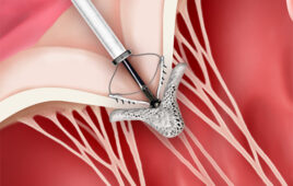
“On laparoscopic and robotic surgical devices, sensors are integral on the tips of these so that the surgeon can gain pressure feedback. The process of cutting into tissue can vary depending on the tissue characteristics, the type of access the surgeon has, and the mode of energy being applied, all of which depends on the type of laparoscopic or robotic tool used. Sensors have to be able to recreate improved levels of ‘sensing feedback’ so the surgeon can maintain the ‘depth/feel’ of the surgical process,” Molin adds.
A growing adoption of Parylene is in “smart” prostheses. Smart prosthetic lower limbs, feet and hands are taking sensors to a new level. These incorporate intelligent electronics, micro sensors and robotics into ankles, feet, wrists, hands and fingers that mimic the real appendages as closely as possible. Parylene protects the sensors while ensuring efficient signal transmission.
“Sensors in ankle or foot prosthetic coordinate position and angle with the person’s gait. For upper extremities they translate how much pressure to put in a hand grip, sending signals back to the person fitted with the device so they can learn to better utilize their new appendage. MEMs sensors are used as gyroscopes for position and speed, and more. This is a very complex array of sensors that must perform without error, and do so with high reliability.”
Designing for Parylene
Because sensors are continually shrinking in size, the integration of Parylene during the design phase can be critical. For example, sensors often need to be connected to something. That contact point needs to remain free of coating. Often, those paths or areas are extremely small. Technologies over the years have been developed to mask and de-mask these extremely small areas, but this may take specialized efforts if done after the design is finalized.
Molin explains, “Designers typically look at device protection at the prototype stage. That’s fine, but if they can plan for protection earlier, input from a conformal coatings provider might make the design process and resulting protection more effective. For example, certain connectors require special masking processes before coating and require de-masking steps post-coating. When connectors are numerous and/or on both sides of a board, labor and material costs increase.
“Because Parylene is applied as a vapor, using a gas-tight connector is one simple example of how a designer could benefit from designing with the end protection in mind. Not only does this sort of communication give the Parylene provider the ability to help with planning for efficient and cost-effective Parylene use, but it is also the best way to decide if Parylene is the best coating for the application.”
Challenges With Parylene
Parylene does present challenges as far as application and usage. One is rework. “Masking and de-masking are different than rework,” says Molin. “To mask/de-mask a component means you are preventing Parylene from entering a certain area. However, if you coat a board that has five different components mounted on it and one of those components fails, to replace that single component would require Parylene rework. Molin added, “To rework Parylene isn’t the easiest task, but it can be done. One method most commonly used is micro–abrasion, another is a plasma etch type process. Parylene is not soluble in solvent, acids or bases, which is a great benefit as a coating, but that also means that it cannot be removed by any known chemical,” says Molin.
While Parylene providers have made the coating process compatible with most substrates, there are some actual device assemblies and applications where the use of Parylene would not be ideal. One example would be an assembly where coated portions of the device rhythmically moved against each other with every beat of the heart. Because Parylene is a polymer, it does not provide a truly “hard” surface; thus over time, the Parylene would eventually wear away. According to Molin, “Parylene can often withstand tens of thousands of cycles, but that’s not nearly enough durability for this particular type of long-term use.”
Applying Parylene presents another challenge. Molin said that while companies can buy equipment and do the process in-house, the learning curve is significant and setting up the entire process can be costly in terms of systems supporting systems and raw materials. The general coating process is documented in the public domain, but elements of the process are considered an art and considered intellectual property to providers.