by Dr. Geoff Shannon, Miyachi America
It is a fact of life that components are getting smaller and smaller, especially in the medical, automotive and electronics markets. New micromachining technology, including advanced laser systems with superior beam quality, can give results similar to traditional machining technologies, but faster and more flexibly. The laser systems used for micromachining are called laser markers because they typically perform marking or engraving operations as opposed to cutting. Fiber marker technology can be two to three times less expensive than standard technology.
High volume manufacturers looking to meet miniaturization machining challenges while reducing costs can use the single mode fiber marker to achieve excellent results on a range of materials, including steel, nickel, titanium, silicon, aluminum, and copper. The method should be considered when updating or replacing electric discharge machining (EDM) equipment, as well when 532- and 355-nm lasers are normally considered in a new process.
Seeing the result without details
Micromachining refers to making small features using standard machining operations such as drilling, cutting, scribing, and slotting—but on a smaller scale. There is no official scale for determining when an operation is considered micromachining, but a rule of thumb is that the features cannot be seen easily with the naked eye. In other words, you might have no idea what was done to the material to get a particular effect. For example, if you drilled 50-µm holes in a piece of copper you would see light, but would not be able to see how big or small the holes were that are letting light through.
The right tool for the job
Working successfully at such a small scale requires the right tool and operating knowledge to achieve the desired results, in terms of both quality and material removal speed.
For example, Miyachi America recently introduced the LMF2000-SM single mode fiber laser marker, which enables micromachining of fine detail dimensionally and at an excellent removal rate.
The laser marker features extremely high beam quality, having a M2(measure of beam quality) of less than 1.3. It can produce a focused optical spot size down to 20 µm, making it suitable for scribing and cutting alumina, silicon, copper, and aluminum foils, among others. In addition, the use of selectable pulse width waveforms with different pulse widths and peak power characteristics enables tuning of the removal rate and quality of the feature surface.
This independent control of pulse width and peak power with pulse frequency offers clear advantages of control and process tunability compared to traditional q-switched lasers that offer fixed pulse width/peak power settings as a function of q-switch frequency. The scan head that rapidly moves the laser is also a key part of the system and needs to provide sufficient high-speed movements with suitable repeatability and accuracy.
Fiber laser micromachining technology can be used in selective plating removal for solder barrier, solar cell scribing and hole drilling, hole drilling of stainless steels for medical hypo tubes and fluid flow control systems, and cutting of sub 0.02-in. thick metals for fast part prototyping.
A comparison to other technologies
Single mode fiber laser markers can be used as an alternative to more costly micromachining technologies, including sinker EDM equipment, or 532 and 355 nm Nd:YVO4 lasers.
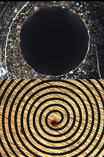
For example, in Figure 1, we see how the technology could be used as a replacement for sinker EDM machines. The picture on the left shows the drilling of a 150-µm hole, ±10 µm in 200-µm thick steel, with no post processing. The minimal amount of debris and tight hole tolerance was achieved in 50% of the time taken by sinker EDM equipment.

Figure 1 – Two 0.006-in. diameter holes drilled in 304L stainless steel demonstrate how fiber laser marking can replace sinker EDM machines. On top is a 0.01-in. thick precision flow device with a hole diameter tolerance of ± 0.0005-in. Below is a spiral with 100-μm wide elements machined into 0.002 in. thick copper
In addition, because the laser marker offers a working XY area, multiple parts can be completed in a single loading operation, as opposed to a one up loading on the sinker machine. This advantage makes the fiber laser marker return on investment (ROI) even more compelling. The fiber laser can process difficult materials such as thin sheet material and foils. Figure 1 also shows a spiral with 100-µm wide elements machined in 50-µm thick copper foil.
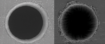
Figure 2 shows a comparison of drilling silicon using a fiber laser marker (left) and a 355 nm UV laser source (right). The UV laser provides a better quality, but the fiber laser results are good enough for this application, offering sufficient quality for “fitness for purpose.” The fiber laser was also 17 times faster than the UV laser and 50% of the cost.

Figure 2 – Comparison between fiber
laser marker, left, and UV laser, right.
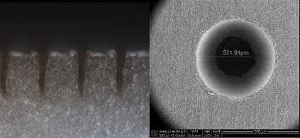
Figure 3 compares the quality of holes drilled with a 20W single fiber laser (left) and 5W 355 nm laser (right) in 0.008-in. stainless steel in the same processing time.
Single mode fiber laser offers high finesse and machining control. For example, it is like taking material that is 1⁄4 the width of a human hair and leaving only about 1⁄10 of a human hair after micromachining.

Figure 3 – Quality comparison between single fiber laser, left and 355 nm laser, right.
Ceramic is another commonly used material in microelectronics, and a 355 nm laser is typically used for scribing and drilling of ceramic materials. Figure 4 demonstrates that the fiber laser marker can avoid micro cracking for a variety of features in ceramic materials.

Figure 4 – Micro cracking, left, can be avoided with the use of fiber laser marking, as seen by the smooth cut on the right.
Many applications require (or can benefit from) the laser’s capability to selectively remove platings or coatings on metals, ceramics and even plastics. Fiber laser machining techniques have shown good results in micromachining solder barriers or solder dams, thin film resistor/capacitor trimming, and active layer removal in battery foils for welding purposes. This selective and tailored layer removal process is usually impossible during component or part production process, because masking the area is simply not feasible.
The laser is useful in selecting a circuit’s exact resistance value. It is excellent when used for resistance or capacitance trimming, as part of a dynamic iterative removal and measure tuning process in which removal areas may change from component to component.

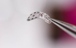
Figure 5 – Fiber laser for solder barriers. Closeup of a single connector on a carrier strip is shown at left, while a gold-coated plastic part is at right. Photo courtesy of SPI Lasers LLC.
Figure 5 shows two examples of solder barriers created using fiber laser. For each part, the laser selectively removes the gold layer. After a gold coating, it can be used to selectively remove material.
Miyachi America
www.miyachiamerica.com


