Medical Design and Outsourcing

  • Home
  • Medical Device Business
    • Mergers & Acquisitions
    • Financial
    • Regulatory
  • Applications
    • Cardiovascular
    • Devices
    • Imaging
    • Implantables
    • Medical Equipment
    • Orthopedic
    • Surgical
  • Technologies
    • Contract Manufacturing
    • Components
    • Electronics
    • Extrusions
    • Materials
    • Motion Control
    • Prototyping
    • Pumps
    • Tubing
  • Med Tech Resources
    • Subscribe to Print Magazine
    • DeviceTalks Tuesdays
    • Digital Editions
    • eBooks
    • Manufacturer Search
    • Medical Device Handbook
    • MedTech 100 Index
    • Podcasts
    • Print Subscription
    • The Big 100
    • Webinars / Digital Events
    • Whitepapers
    • Video
  • 2022 Leadership in MedTech
    • 2022 Leadership Voting!
    • 2021 Winners
    • 2020 Winners
  • Women in Medtech

Virginia Tech Engineers Develop New Process For Creating Micro- And Nanostructures On 3-D Materials

October 31, 2016 By Rosaire Bushey, Virginia Tech

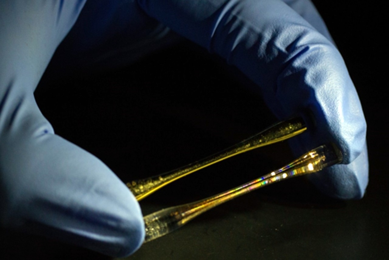
Gold-coated glass shows structural coloration, which happens due to the diffraction of light off surface nanostructures. (Credit: Virginia Tech)

A process for creating micro- and nanostructures on 3-D objects holds great promise to usher in new nano-enabled applications in advanced materials and biotechnology.

The work, published in the journal Nanoscale in July, drastically reduces costs while speeding the production process by four to six orders of magnitude, compared to current state of the art techniques, according to Virginia Tech mechanical engineering doctoral student Zhou Ye; his advisor, Associate Professor Bahareh Behkam; and their collaborator, Associate Professor Amrinder Nain. 

Their process, called Spun-Wrapped Aligned Nanofiber (SWAN) lithography, can fabricate micro- and nanostructures on the entire surface of any 3-D object by applying polymer fiber that is about 500 times smaller than the diameter of human hair over an object, followed by etching areas of the object not covered by the fiber and then removing the fiber itself, thus resulting in a nanotextured gold surface.

Gold film is widely used in biosensing applications due to its nonreactive and conductive nature. With SWAN lithography’s ability to pattern the entire 3-D object independent of curvature, the sensing area along with the signal-to-noise ratio are substantially increased. The process works on all 3-D objects irrespective of their geometry, thereby overcoming a major limitation of current methods, which work only on simple geometries (such as cylindrical objects) or flat surfaces.

In addition to its ability to pattern complex-shaped objects, SWAN lithography also has three additional characteristics that, in the words of Behkam, “make the potential for the process, expansive. The first is that SWAN lithography can be applied to a wide variety of object shapes of varying curvatures, and be done at both micro- and nanoscales, something electron beam lithography (EBL) and focused ion beam milling (FIB) can’t do,” Behkam said. “Second, we have reduced the costs considerably; and finally, the time it takes to texturize an object is orders of magnitude faster compared to other methods.”

Behkam contends the current commercially available systems for creating nanostructures typically take 10,000 to 1 million times as long. That means what SWAN lithography can do in one minute, the others would spend 166 hours or 694 days to accomplish.

“Really, it allows us to explore a large variety of application areas. We are especially interested in health care-related technologies,” Behkam said. “We are working to engineer nanocomponents that work with biologic components. For example, in implantable medical devices, microbial infections are not only associated with increased mortality but are also significant contributors to the emergence of antibiotic resistance traits. With increased life expectancy, we are likely to see an increase in the use of short- and long-term implantable biomedical devices. This represents a growing unmet medical need to counter microbial biofilm-associated infections. Current treatment for biofilm-associated infections typically involve a combination of surgical replacement of the implant and long-term antibiotic therapy, which incurs high health-care costs and remains controversial because compelling evidence of their effectiveness is lacking. SWAN lithography enables engineering of micro/nano-scale topological cues on the surface of medical implants to mitigate biofilm formation, allowing a far-superior function and safety.”

In addition to medical applications, the SWAN lithography process also allows functionality to be built into other products, including nanosensors for photonic and plasmonic applications.

Currently, Behkam and her team are speaking with industry to further develop the patent-pending technology and bring it to the next step for wide-scale use in everything from camera lenses and aircraft wings, to ship hulls, solar panels, and biomedical devices and implants. 

Related Articles Read More >

Connected device design for the real world: Managing the development process
A portrait of ResMed President and COO Rob Douglas
ResMed finds a solution to semiconductor shortage, as well as some humor in it
Johnson & Johnson Office of Digital Innovation Leader Peter Schulam
Imagining the future of cloud-connected medical devices with Johnson & Johnson leaders
Withings Body Scan
Withings plans launch for Body Scan smart scale platform

DeviceTalks Weekly.

August 5, 2022
DTW Medtronic's Greg Smith lays out supply chain strategies
See More >

MDO Digital Edition

Digital Edition

Subscribe to Medical Design & Outsourcing. Bookmark, share and interact with the leading medical design engineering magazine today.

MEDTECH 100 INDEX

Medtech 100 logo
Market Summary > Current Price
The MedTech 100 is a financial index calculated using the BIG100 companies covered in Medical Design and Outsourcing.
DeviceTalks

DeviceTalks is a conversation among medical technology leaders. It's events, podcasts, webinars and one-on-one exchanges of ideas & insights.

DeviceTalks

New MedTech Resource

Medical Tubing

Enewsletter Subscriptions

Enewsletter Subscriptions

MassDevice

Mass Device

The Medical Device Business Journal. MassDevice is the leading medical device news business journal telling the stories of the devices that save lives.

Visit Website
MDO ad
Medical Design and Outsourcing
  • MassDevice
  • DeviceTalks
  • MedTech100 Index
  • Medical Tubing + Extrusion
  • Medical Design Sourcing
  • Drug Delivery Business News
  • Drug Discovery & Development
  • Pharmaceutical Processing World
  • R&D World
  • About Us/Contact
  • Advertise With Us
  • Subscribe to Print Magazine
  • Subscribe to E-newsletter
  • Attend our Monthly Webinars
  • Listen to our Weekly Podcasts
  • Join our DeviceTalks Tuesdays Discussion

Copyright © 2022 WTWH Media, LLC. All Rights Reserved. The material on this site may not be reproduced, distributed, transmitted, cached or otherwise used, except with the prior written permission of WTWH Media LLC. Site Map | Privacy Policy | RSS

Search Medical Design & Outsourcing

  • Home
  • Medical Device Business
    • Mergers & Acquisitions
    • Financial
    • Regulatory
  • Applications
    • Cardiovascular
    • Devices
    • Imaging
    • Implantables
    • Medical Equipment
    • Orthopedic
    • Surgical
  • Technologies
    • Contract Manufacturing
    • Components
    • Electronics
    • Extrusions
    • Materials
    • Motion Control
    • Prototyping
    • Pumps
    • Tubing
  • Med Tech Resources
    • Subscribe to Print Magazine
    • DeviceTalks Tuesdays
    • Digital Editions
    • eBooks
    • Manufacturer Search
    • Medical Device Handbook
    • MedTech 100 Index
    • Podcasts
    • Print Subscription
    • The Big 100
    • Webinars / Digital Events
    • Whitepapers
    • Video
  • 2022 Leadership in MedTech
    • 2022 Leadership Voting!
    • 2021 Winners
    • 2020 Winners
  • Women in Medtech