Across industry, there is a concerted and accelerating trend towards miniaturization, and nowhere more so than in the medical device sector, where demand for minimally invasive diagnostic and treatment devices is growing exponentially. Very often these smaller and smaller devices are becoming more and more complex, and the search is on for medical device OEMs to locate manufacturing processes that can keep up with their exacting requirements. When it comes to the manufacture of metal precision medical devices, the role of photo etching is growing in the medical sector, due to its unique process characteristics, and the fact that in many instances it is the only process that can achieve the results demanded in what are sometimes extreme and safety critical applications. This article looks at the photo etching process, and analyses its use in the medical device sector through reference to some real time industrial case studies. Photo etching is stimulating innovation in medical product design as it pushes at the boundaries of what has previously been perceived as possible in metal manufacturing.
Broadly speaking, the $130 billion medical device sector is likely to be affected by three key trends in the short to medium term. First, the drive for technology focused on earlier and more accurate diagnostics; second, advances in IT/e-health technologies; and third — and perhaps most importantly — the miniaturization of devices.
In the medical device sector, OEMs are constantly searching for new and innovative solutions, key market drivers being the ability to produce efficient and ever smaller devices that are cost-effective to produce, and that can be manufactured in volume and to strict time-to-market parameters. Also of vital concern is the fact that these novel devices are often developed for highly regulated sectors, requiring that any partner in device development is also equipped with the knowledge necessary to navigate the regulatory hoops in a timely fashion, while at the same time ensuring compliance with an array of quality standards.
Without a doubt, across industry in general it is the medical device sector that is at the forefront of the drive towards miniaturization. In the medical device industry, the usual advantages of making smaller parts (such as reduced material usage, reduced weight, and reduced cost) are exacerbated by the requirement for less invasive treatments. In addition, the opportunities for diagnosis and treatment that are available if functioning devices can be swallowed, ingested, or inserted in the body are huge, and constantly stimulate innovation in the micro manufacturing field.
The heat is on for medical device OEMs to maintain profitability despite downward pressure on prices, and this will only be achieved as time progresses through the development of innovative products that will fulfil the ever more exacting requirements of end-users. Demand will increasingly be for versatile devices that will embrace the potential for “smart” diagnostics and treatment presented by the proliferation of so-called “big data”; and devices that provide cheap alternatives to traditionally used but expensive diagnostic and therapeutic devices.
In a nutshell, demand for minimally invasive curative and diagnostic procedures is growing exponentially as patients and medical service delivery organizations seek to reduce operation and recovery times, and increase the accuracy of diagnosis. Because of this, over the last decade, medical product manufacturers have been designing (and seeking to manufacture) smaller and smaller components with more and more complex and minute features. Couple this with the overarching demand from patients and healthcare providers to rationalize the costs associated with medical treatment, and medical device OEMs are constantly on the lookout for cost-effective and efficient manufacturing processes.
Choice of Process and Partner
Very often, the personnel within medical device OEMs that are developing such new and innovative products are medical scientists, not medical product manufacturers. So saying, they need to be able to access the best-fit manufacturing processes, and this is usually done by engaging specialist precision engineering companies that can take original design intent and convert it into viable and marketable products quickly and cost-effectively. The emphasis is on partnership with qualified manufacturing professionals, but also key is the selection of a partner that is expert in a manufacturing process that is compatible with industry demands.
When it comes to metal parts and components, an increasing number of medical device OEMs are assessing and embracing the use of photo etching as the manufacturing process of choice. Let’s look at some of the key aspects of this technology that make it such a good fit for the medical device sector, and how it measures up against other available technologies.

Coupled with the fact that photo etching uses easily re-iterated and low-cost digital tooling, it provides a cost-effective, highly accurate, and speedy manufacturing alternative to traditional machining technologies such as metal stamping, pressing, CNC punching, and laser and water-jet cutting.
Traditional machining technologies can produce less than perfect effects in metal at the cut line, often deforming the material being worked, and leaving burrs, heat-affected zones, and recast layers. In addition, they struggle to meet the detail resolution required in the ever smaller, more complex, and more precise metal parts that medical device OEMs require. There are instances — typically when an application requires multiple millions of parts and absolute precision is not a priority — when these traditional processes may be the most cost-effective. However, if OEMs require runs up to a few million, and precision is key, then photo etching with its lower tooling costs is often by far the most economic and accurate process available.
Another factor to consider in process selection is the thickness of the material to be worked. Traditional processes tend to struggle when applied to the working of thin metals, stamping and punching being inappropriate in many instances, and laser and water cutting causing disproportionate and unacceptable degrees of heat distortion and material shredding respectively. While photo etching can be used on a variety of metal thicknesses, one key attribute is that it can also work on ultra-thin sheet metal, even as low as 10 micron foil.
It is in the manufacture of intensely complex and feature-rich precision parts that photo etching really finds its perfect application, as it is agnostic when it comes to shapes and unusual features in products to be manufactured. The nature of the process means that feature complexity is not an issue, and in many instances, photo etching is the only manufacturing process that can accommodate certain part geometries.
Active in the field for many decades, Precision Micro is constantly pushing the boundaries of what is possible in the process, making advances in etchant chemistry, and developing the process to embrace more and more metals, and enhance accuracy for its customers. It is this pre-eminence that has led numerous world-renowned medical device OEMs to partner with Precision Micro in the manufacture of often complex and safety critical products.
Medical Device Case Studies:
 Micro Filters
The nature of the photo etching process makes it ideally suited to the manufacture of precise, reliable, and cost effective meshes and filters In a variety of applications, not only can photo etching be the most cost-effective and accurate fabrication technology for intricate meshes and filters, but its unique process characteristics actually assist in the stimulation of innovative product designs impossible to manufacture using conventional machining or metal cutting technologies.
When applied specifically to the manufacture of customized meshes and filters, photo etching is characterized by a number of process advantages. Lead times are reduced dramatically, as are contingent costs, as tooling set up and iterations (which are often necessary) are quick and relatively simple. Being digital, the tooling for photochemical etching can be manipulated on screen with ease and take a matter of hours rather than the days or weeks that would be expected with traditional processes.
Also, of particular interest to meshes, special features and various aperture shapes can be incorporated in a single mesh without any cost penalty. Using the photo etching process, Precision Micro can incorporate etched meshes up to 1500 mm by 600 mm which is unique in the industry, and a wide range of materials can be processed. Varying bar sizes and open area ratios can be incorporated to control flow rates across the mesh, and something that appeals to medical device design engineers is that the photochemical etching process allows for far greater open areas than is possible using alternative processing technologies due to its ability to produce tiny and intricate wire sizes.
When compared with meshes that are woven, the single-part meshes and grids that are produced via photo etching are characterized by their consistent cross-sectional thickness and accuracy of aperture shapes and sizes. Also, as they are manufactured from a single piece of metal, they are slimmer, have greater integrity, are robust when being handled, and the exhibit better electrical properties with no risk of poor contacts at the weave intersect.
Custom borders can also be added for additional strength.
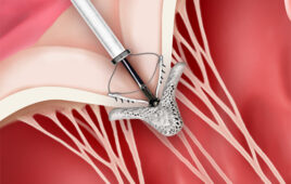
For one particular medical device OEM, Precision Micro worked on a blood filtration product that had been frustrated in its attempts to produce a micro filter using alternate technologies and service providers (Figure 2). Before coming to Precision Micro, the company had made the filter using a hugely expensive, time-consuming, and — due to the production of burrs on the underside of the component — inefficient and ineffective laser fabrication process. Precision Micro’s job was to pierce a 78 mm diameter, 50 micron thick stainless steel disc with over 130,000 apertures, each being 100 microns in diameter on a staggered pitch of 200 microns with a maximum allowable tolerance of +/- 10 microns against a standard tolerance for photochemical etching of +/- 25 microns.
As the photochemical etching process (unlike the previously used laser process) allowed for the etching of all 130,000 holes simultaneously, Precision Micro was able to not only provide burr and stress free filters, but they were produced in a fraction of the time and therefore afforded the OEM a cost-effective route to mass production.
 Medical Saw Blade
Traditionally, such sharp-toothed blades have been manufactured using laser technology followed by precision grinding in order to achieve the required tooth off-set. By combining its Laser Evolved Etch Process (LEEP) with advanced wire erosion techniques, Precision Micro has improved part quality in a more economic and efficient manner.
Tooth off-set and blade topography is achieved using the depth-etch technique with dissimilar patterns on each side of the blade. An etch resist is applied to both surfaces and a pattern is exposed on each side simultaneously using Laser Direct Imaging. This guarantees top/bottom pattern alignment. The exposed plate is then developed, revealing the metal to be etched away. The depth-etch process erodes the metal from both sides simultaneously, generating the required topography but leaving the blade securely within the overall metal sheet.
Depending on the part and the material type, photo etching can become a little uneconomical above 1.5mm thicknesses due to the amount of time involved in the chemistry. Because of this, Precision Micro profiled the blades using Advanced Wire EDM. Even though it meant a second operation, it was a far more cost-effective solution for the customer.
Sheets are stacked and machined to produce hundreds of blades in a single cycle. The process can achieve tolerances of <±5µm that cannot be achieved using other metal cutting techniques.
A feature of the Advanced Wire EDM process is its ability to generate parallel sidewalls with accuracy more than sufficient to create the ultra-sharp tooth profile required. Rigorous process validation, from the design stage through to commercial production, has shown this process route to be capable of consistently delivering quality product.
The blades are manufactured from a hardened, Sandvik martensitic stainless steel, characterized by its very good corrosion resistance, high toughness, and excellent fatigue strength. Being an ambient temperature process, the blades are not subject to thermal stress, and all the original material properties are maintained.
This Precision Micro “process combination” utilizes all digital tooling, making it economical to manufacture the numerous versions of bone saw blades that have been optimized for each specific procedure. The same process route is used to produce prototypes and volume parts, an essential requirement when seeking medical device classification and certification.
 Implantable Screening Cans for Pacemakers
Precision Micro has developed its own dielectric coating process for the inside of shielding cans where the possibility of arcing exists between circuitry and the grounded shielding can, which is especially useful for medical device OEMs involved in the manufacture of active electronic medical devices. Arcing can occur as a result of turn-on spikes or surges (electromagnetic pulses) caused by external stimuli, and can obviously be very damaging to such electronic medical devices.
It is possible for the insulative coating to be applied selectively to inside surfaces of the shielding can considered most susceptible to arcing, enabling cans to be designed to fit in with reduced profile requirements favored increasingly by electronics designers.
The ability to reduce the overall height of a can makes it better able to meet the miniaturization requirements of modern electronics assemblies and can also improve attenuation by minimizing the linear dimension of apertures which in broad terms governs the efficiency of the shielding can.
Branded “MicroSafe”, this exceptionally even coating is pinhole free and has no detrimental effect on the shielding efficiency of the formed can. Adhesion to the substrate metal (usually nickel silver) is excellent, and the upper operational temperature is claimed to be in excess of 260 degrees C.
 Photochemical Etching of Flat Springs for Hearing Aid Application
The key attributes of photo etching — namely its ability to produce parts in high volumes that are burr and stress free — made it an ideal choice for the manufacture of flat springs required by a medical device OEM with a hearing aid application. For this application, material performance and integrity was critical.
In addition, the extremely thin nature of the springs — ranging as they do from 38-100 microns — coupled with their small overall size (4mm x 8 mm), introduced other manufacturing challenges. It was vital that these parts exhibited clean profiles, which was achievable through the photo etching process, and parts that were burr free. For mass production of these parts, photo etching also allowed a high yield from the sheet of material being worked, which made the process extremely cost-effective when compared with other technologies.
The thin flat springs used in the hearing aid had to be produced with extremely low tolerances, and for this application, Precision Micro achieved the standard tolerance of +/- 25 microns. To accommodate these fine tolerances, various tooling iterations were required which was possible to do cost-effectively with the photo etching process as the tooling is digital. This means that multiple tooling redesigns can be produced not only much more cheaply than processes that require physical metal tooling, but also extremely quickly.
The CAD team at Precision Micro is staffed by highly experienced experts in the area of digital tooling for the photochemical etching process with a combined experience of over 50 years. Such in depth understanding of the process is one of the reasons that Precision Micro is one of the world’s leading exponents of the process. With so much of the success of mass production of parts using photo etching — such as the flat springs in this particular hearing aid application — being down to the expertise at the digital tooling stage (applying the experience of the tooling team to the specifics of a particular product design) it is important that medical device OEMs partner with their chosen photo etching provider early in the design stage in order to maximize the time-to-market savings that are inherent in the process.
 Biosensor for Highlands Biosciences
Highland Biosciences, Duncanston, U.K., creator of leading-edge diagnostics technologies, partnered with Precision Micro to develop and manufacture a miniaturized “tuning fork” biosensor. The component forms an essential part of Highland Bioscience’s proprietary microviscometer, which has the potential to improve the safety of a number of medical procedures by providing results conveniently at the point of need.
With a tight innovation cycle needed, and a reliance on the material properties being unaffected during manufacture, both stamping and laser cutting were ruled out as viable methods of both prototype and production parts.
Instead, photo-etching was chosen using tightly controlled chemistry to selectively remove metal atom by atom with micron accuracy, imparting no stress or burr on the base material. As every biosensor produced required a perfectly clean surface to ensure consistent adhesion of the surface coating, Precision Micro developed a dedicated post-process cleaning operation supported by 100% automated optical inspection.
Both innovation and the advanced etching techniques employed in the production of the biosensor were recognized by the Technology Strategy Board (TSB), the UK’s leading innovation agency, and attracted TSB funding of $1.6 million for a manufacturing development project. This project focused on the mass manufacturing and scale up needed to launch the product, and the biosensor is being readied to make the transition to volume manufacture, expected to reach 50 million components over the next 5 years, utilizing the same digital tooling, and to a quality comparable to parts produced in silicon.
Conclusion
It is the case that throughout history, medical advances have been made due to technological innovation, and in effect, photo etching is just another technological innovation that enables the design, manufacture, and clinical use of groundbreaking medical devices. Not only will the technology allow for the manufacture of complex precision devices, but in many instances it is the only metal processing technology that can cost-effectively and repeatably produce mass produced parts to the standards necessary in many medical applications.
In the U.S. medical device industry (which is learning to live with the increased taxation that was levied on the sale of medical devices in 2013, and with the increased power and purchasing muscle of Group Purchasing Organizations (GPOs)) and indeed all other global health sectors, any technology or manufacturing solution / process that allows for the attainment of product functionality while reducing costs is to be welcomed. It is here that photo etching has such a role to play in this important sector. The use of such cost-effective and sophisticated technologies, healthcare reforms, and a continually aging population will help to mitigate the pressures on the profitability of medical device OEMs.