The Project: To figure out the design and manufacture of microelectronics circuits used inside a complex new artificial spinal disc.
The Solution: Create a miniaturized packaging solution that fits the electronics into a volume of less than two cubic centimeters.
Donald Styblo is vice president of technology at Valtronic USA Inc., 6168Cochran Rd., Solon, OH 44139. Valtronic, which provides custom solutions formedical products ranging from hearing products to implantable biosensors andstimulators, has manufacturing facilities in Ohio, Switzerland, and Morocco.Styblo can be reached at 888-291-9422, ext. 19, or www.dstyblo@valtronic.com.Ric Navarro is vice president of R&D at Theken Disc LLC, 283 E. Waterloo Rd.,Akron, OH 44319. Theken Disc specializes in medical device testing, product development,research, and manufacturing. Navarro can be reached at 330-773-7677, ext 217,or www.rnavarro@thekendisc.com.By Donald Styblo and Ric Navarro
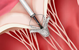
 Theken Disc with an X-ray image of the miniaturized electronics module (click the image to enlarge) |
Theken Disc LLC has partnered with Valtronic USA Inc. to develop an artificial spinal disc to replace damaged human discs. This elastomer/metal disc is being engineered to restore the natural kinematics and dynamics of a spine motion segment and to serve as an alternative to spinal fusion procedures. Additionally, it will have the ability to monitor itself and the patient.
Valtronic is known for its designs and fabrications of miniaturized electronic modules used in both in vitro and in vivo medical products. For this project, its objective was to assist Theken with the electronics design and manufacture of the microelectronics circuits used inside the disc. The embedded microelectronics enable the patient and surgeon to manage the critical post-operative period and to maximize the life of the implant. The project currently is undergoing extensive testing, which will lead to animal implantation this year and human trials next year.
Today’s artificial disc designs replicate range of motion but have no ability to exert force to restore a “neutral” position of a motion segment. Thus, the task is left to the facets, ligaments, muscles, and remaining annulus in the spine. Artificial disc ball and socket designs are orders of magnitude stiffer in compression than the natural human disc and do not absorb energy. The effects of these shortcomings in replicating the natural disc biomechanics are as yet unknown. However, Theken believes it is important to restore the natural kinematics and dynamics of a spine motion segment in its new disc. For the long-term health of soft tissues and facets, the elasticity of the anterior column unit should be restored to normal physiologic ranges.
The Theken Disc is being developed to restore not only the kinematics of the natural disc but also its non-linear elasticity. These restorative forces contribute load-sharing stiffness in six degrees of freedom. To overcome the limitations of a bonded elastomer design, mechanical strain limits are being built into the device, preventing rubber stresses and strains from exceeding endurance limit values in all important motion directions. Also, a proprietary elastomer was developed with improved fatigue performance and other properties essential to survive the high loads of the spine.
Valtronic’s responsibility was to design a miniaturized packaging solution that would fit the electronics into a volume of less than two cubic centimeters — about the size of an index finger to the first joint. The solution has multiple integrated circuits (ICs) performing data acquisition, processing, storage, data transmission, and power management functions. In addition to these components, more than 80 surface-mount components, including crystals, capacitors, and resistors of various sizes and values, were added to the substrate.
The Theken Disc required an extremely complex design that is not only smaller than most in vivo medical devices but also more energy efficient, reliable, and rugged. In addition, testing and qualifying materials are crucial during intermediate and final stages of production as well as in the verification of the manufacturing techniques. Also, test capabilities had to be incorporated into the original designs in a way that the need for increased testing would not unnecessarily burden the final size, cost, performance, production throughput, or reliability.
Valtronic evaluated three types of flip-chip attachment technologies as well as a chip-on-board
direct-die attach assembly technology to satisfy the space and rigid design requirementsof the disc. (For additional evaluation information, see www.valtronic.com.) These were:
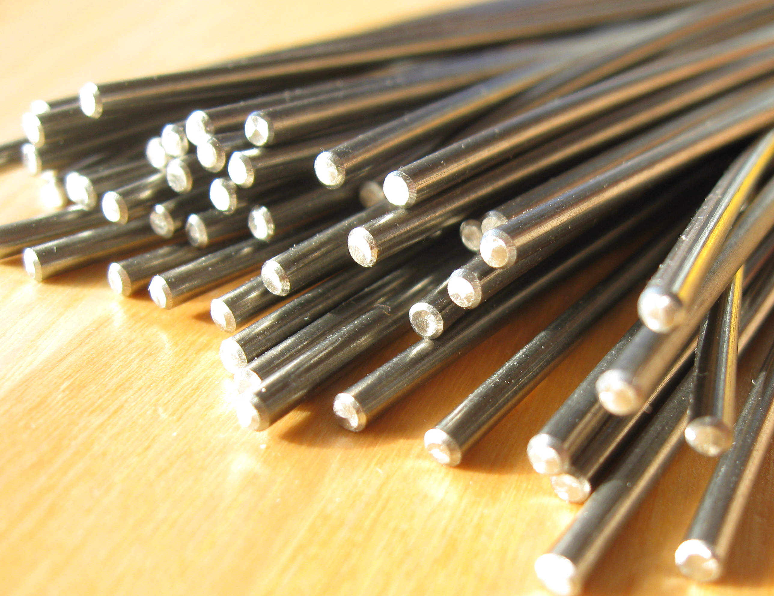
 Gold stud bumps on the IC with an I/O pitch of less than 125 microns |
1. Gold-On-Gold stud-bump flip-chip attachment with non-conductive adhesive (NCA).
2. Soldered (C4) attachment.
3. Conductive adhesive attachment (CAA).
4. Chip-on-board gold wire bonding.
The result of an extensive study compelled Valtronic to utilize a combination of solutions—the Gold-On-Gold NCA flip-chip and the chip-on-board processes as well as surface-mount technology.
The die bumping is to be carried out by a high-speed wire bonding machine leaving gold bumps called stud bumps. This gold stud bumping provides great versatility, and the process can be carried out on either standard wafers or with individual ICs in waffle packs. Gold stud bumping is more economical than the C4 or CAA processes, utilizing off-the-shelf semiconductor devices without additional pad metallizations.
One advantage of the Gold-On-Gold NCA flip-chip process is the low impedance of the contact when the die is pressed onto the surface of the flex board substrate. The bonding pressure required is from 50 to 80 grams per connection. Both sides of the package are then heated to cure the adhesive. Non-conductive adhesive can be cured at temperatures low enough to eliminate the possibility of heat damage. Temperatures of approximately 200°C or lower are required for as little as five seconds. Prior to applying the heat, the assembly can actually be tested electrically. The curing of the adhesive generates an important shrinkage effect that pulls the die and substrate against each other, applying a permanent force to each stud bump that guarantees electrical contact will be maintained over the life of the product.
To qualify Valtronic’s Gold-On-Gold flip-chip process, a daisy-chain ASIC die was designed and fabricated by Valtronic. The daisy-chain ASICs have two types of conductive traces. The larger are current-carrying traces that internally heat up the die under test when a voltage is connected across the two nodes. The smaller are continuity traces that check the continuity of the flip-chip attachment under extreme conditions.
Worst case temperature and humidity cycling tests were conducted on a series of daisy-chain die measuring 12 x 12 millimeters mounted to FR4, BT, and polyimide flex substrates using proprietary adhesive. The test die included four-wire resistance measurement sites that provide for high-accuracy resistance measurements. In addition, extensive temperature and humidity cycling tests were performed using the daisy-chain die mounted to the FR4 substrate in order to investigate the thermal coefficient of expansion and performance of the non-conductive adhesive and gold stud bumps.
 Daisy-chain die contacts |
The temperature test was designed to provide cycling over a range of -40°C to +125°C in order to simulate actual environmental storage and operating temperatures of medical products. Continuity measurements were made after 25, 50, 100, 250, 500, 750, and 1,000 cycles.
Humidity testing at +85°C/85% RH was conducted, and resistance measurements taken at 250, 500, 750, and 1,000 hours of storage.
The temperature cycling tests confirmed that contact resistance stays within 2-3 milliohms of initial values after 1,000 air-to-air thermo cycles of -40°C to +125°C. All contact resistance measurements were made on PC board pins that encircle the die. As a result, resistance measurements for pads toward the center of the die involved longer traces on the FR4 PC board, and the test data reflected these measurements. Changes in resistance versus temperature were found to be similar for contacts in the center of the die as compared to contacts at the edge of the die for temperatures up to approximately 150°C. It was also observed that contact resistance values did not permanently change after repeated temperature cycling but returned to pre-test values.
Test results also showed that the resistance of the contacts at the center of a die is typically within 1.5 milliohms of those at the edge of the die. The differences can be attributed to the increased length of traces in the resistance path of the FR4 PC board. The Gold-On-Gold contact system also demonstrated the ability to maintain electrical integrity after 1,000 temperature cycles. In other words, there was no indication of outright failure of any contacts.
In addition, the possibility of adhesive being trapped between the stud bump and substrate pad surfaces was shown to be nil. The stud bump crushed as expected during bonding, and there was no indication of adhesive between bumps and substrate pads.
Based on these findings, it was concluded that the non-reactive chemistry of the Gold-On-Gold contact system maintains consistent conductive properties over the range of -40°C to +125°C. Another conclusion was that any stresses due to thermal mismatches have no lasting effect after 1,000 temperature cycles. Concerning storage in a prolonged high-temperature/high-humidity environment, a rise in contact resistance of approximately 2 milliohms was observed per I/O contact after 1,000 hours at 85%RH/85°C.
A final note on the use of flip-chip technology in miniaturized electronics: the factors that limit the level of miniaturization achievable with the Gold-On-Gold flip-chip system are the circuit board’s quality and consistency. The current state of Gold-On-Gold flip-chip technology supports chip placement to tolerances as small as ۫ µm with ۯ µm being routine. Furthermore, Gold-On-Gold flip-chip technology provides for extremely tight control of all aspects of manufacturing, which permits closer chip placement, sequential multiple chip attachments, device testing during assembly, and other advantages unique to this process.
ONLINE
For additional information on the products and technologies discussed in this article, see Medical Design Technology online at www.mdtmag.com and the following websites:• www.valtronic.com• www.thekendisc.comTheken Disc with an X-ray image of the miniaturized electronics moduleGold stud bumps on the IC with an I/O pitch of less than 125 micronsDaisy-chain die contacts