Scientists from Russia and Australia have put forward a simple new way of counting microscopic particles in optical materials by means of a laser.
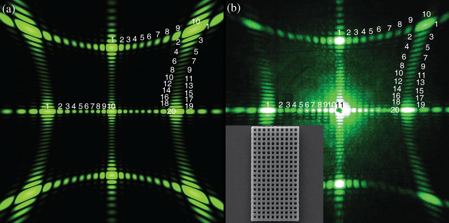
A light beam passing through such a material splits and forms a characteristic pattern consisting of numerous bright spots on a projection screen. The researchers found that the number of these spots corresponds exactly to the number of scattering microscopic particles in the optical material. Therefore, the structure and shape of any optical material can be determined without resorting to the use of expensive electron or atomic-force microscopy.
The production of optical circuits requires devices that can amplify optical signals, bring them into focus, rotate and change their type of motion. Ordinary lenses cannot cope with these tasks at nanoscale, so scientists are working with artificial optical materials; photonic crystals and metamaterials, which can control the propagation of light in most extraordinary ways. However, fabricating optical materials with desired properties is a laborious process that needs constant improvement.
The scientists from ITMO University, Ioffe Institute, and Australian National University for the first time suggested analyzing the structure of photonic crystals using optical diffraction method, that is, by looking at the light pattern generated while the sample is exposed to a laser beam. The number of these spots is equal to the number of scattering microscopic particles in the sample structure. Previously, such small particles could only be seen and counted with powerful and expensive electron or atomic-force microscopes.
“The light senses heterogeneity,” says Mikhail Rybin, senior researcher at the Department of Nanophotonics and Metamaterials at ITMO University. “Depending on the shape and relative position of the scatterers, the light wave continues to propagate differently behind the sample. In other words, the structure of the sample affects the diffraction pattern, which will be projected on the screen. We found out that looking at the pattern, it is possible to determine the precise number of scatterers in the material. This helps understand not only the type of the sample lattice (square, triangular), but also to establish its structure (20 to 20 particles, or 30 to 15) just by counting light spots on the screen.”

Experimentally obtained and simulated diffraction patterns for a sample. (Credit: ITMO University)
The new method has already enabled scientists to investigate the transition between two main classes of optical materials: photonic crystals and metasurfaces. In both classes, the scattering particles (rings, balls, cylinders of 200-300 nanometers) are arranged in a flat lattice. However, in case of two-dimensional photonic crystal, the light perceives the sample as a set of separate particles.
Therefore, passing through it the light generates a fancy pattern on the screen behind the sample. In case of metasurfaces, the light perceives the sample as homogenous. The screen shows only one bright spot indicating that the scattering particles are located close enough to each other, such that the light does not see them as separate particles and passes through the sample without splitting.
In order for the light beam to pass through a metasurface, the distance between the particles has to be smaller than the wavelength of light. Calculations show that for some structures it is needed to produce a lattice where the distance between particles is two to three times smaller than the wavelength of light. Often, however, meta-properties can manifest themselves at larger distances between the particles. It is important to find the maximum allowable distance, since reducing the structure by one single nanometer makes the technology more expensive.


